Data Sheet PU10322EJ01V0DS
3
NE5511279A
ELECTRICAL CHARACTERISTICS
(TA
= +25?C, unless otherwise specified, using our standard test fixture)
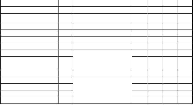
Parameter
Symbol
Test Conditions
MIN.
TYP.
MAX.
Unit
Gate to Source Leak Current
IGSS
VGS
= 6.0 V
?
?
100
nA
Drain to Source Leakage Current
(Zero Gate Voltage Drain Current)
IDSS
VDS
= 8.5 V
?
?
100
nA
Gate Threshold Voltage
Vth
VDS
= 4.8 V, IDS
= 1.5 mA
1.0
1.5
2.0
V
Thermal Resistance
Rth
Channel to Case
?
5
?
?C/W
Transconductance
gm
VDS
= 3.5 V, IDS
= 900 mA
?
2.3
?
S
Drain to Source Breakdown Voltage
BVDSS
IDSS
= 15 ?A
20
24
?
V
Output Power
Pout
f = 900 MHz, VDS
= 7.5 V,
38.5
40.0
?
dBm
Drain Current
ID
Pin
= 27 dBm,
?
2.5
?
A
Power Added Efficiency
?add
IDset
= 400 mA (RF OFF)
42
48
?
%
Linear Gain
GL
Note
?
15.0
?
dB
Output Power
Pout
f = 460 MHz, VDS
= 7.5 V,
?
40.5
?
dBm
Drain Current
ID
Pin
= 25 dBm,
?
2.75
?
A
Power Added Efficiency
?add
IDset
= 400 mA (RF OFF)
?
50
?
%
Linear Gain
GL
Note
?
18.5
?
dB
Note
Pin
= 5 dBm
DC performance is 100% testing. RF performance is testing several samples per wafer.
Wafer rejection criteria for standard devices is 1 reject for several samples.

发布紧急采购,3分钟左右您将得到回复。
相关PDF资料
NE5520379A-A
MOSFET LD N-CHAN 3.2V 79A
NE552R479A-A
MOSFET LD N-CHAN 3V 79A
NE5531079A-A
FET RF LDMOS 460MHZ 30V 79A
NE55410GR-AZ
MOSFET LD N-CHAN 28V 16-HTSSOP
NE650103M-A
MESFET GAAS 2.7GHZ 3M
NHD-0108BZ-FSY-YBW-3V3
LCD MOD CHAR 1X8 Y/G TRANSFL
NHD-0108BZ-RN-GBW
LCD MOD CHAR 1X8 NO REFL
NHD-0108BZ-RN-YBW-33V
LCD MOD CHAR 1X8 Y/G REFL STN
相关代理商/技术参数
NE5511279A-T1
制造商:California Eastern Laboratories (CEL) 功能描述:Trans RF MOSFET N-CH 20V 3A 4-Pin Case 79A T/R
NE5511279A-T1A
制造商:California Eastern Laboratories (CEL) 功能描述:Trans RF MOSFET N-CH 20V 3A 4-Pin Case 79A T/R 制造商:California Eastern Laboratories 功能描述:Trans RF MOSFET N-CH 20V 3A 4-Pin Case 79A T/R
NE5511279A-T1-A
功能描述:射频MOSFET电源晶体管 UHF Band RF Power RoHS:否 制造商:Freescale Semiconductor 配置:Single 晶体管极性: 频率:1800 MHz to 2000 MHz 增益:27 dB 输出功率:100 W 汲极/源极击穿电压: 漏极连续电流: 闸/源击穿电压: 最大工作温度: 封装 / 箱体:NI-780-4 封装:Tray
NE5511279A-T1A-A
制造商:CEL 制造商全称:CEL 功能描述:7.5 V UHF BAND RF POWER SILICON LD-MOS FET
NE5512
制造商:PHILIPS 制造商全称:NXP Semiconductors 功能描述:Dual high-performance operational amplifier
NE5512D
制造商:PHILIPS 制造商全称:NXP Semiconductors 功能描述:Dual high-performance operational amplifier
NE5512N
制造商:NXP Semiconductors 功能描述:Operational Amplifier, Dual AMP, Bipolar, 8 Pin, Plastic, DIP
NE5514
制造商:PHILIPS 制造商全称:NXP Semiconductors 功能描述:Quad high-performance operational amplifier
